
The CNMS offers two Oxford Instruments PlasmaLab System 100 plasma dry etchers used to etch a wide variety of thin films and materials. One system is primarily used to etch silicon-based films and materials, the other is primarily used to etch metals and most other less common materials that can be chemically and/or physically etched.
The Inductively Coupled Plasma (ICP) Deep Reactive Ion Etchers (DRIE) utilize two RF generators. The first generator produces a remote ICP plasma, and the second biases the remote plasma against the sample to be etched. The etchers are load lock equipped, high vacuum chambers with typical etch process pressures ranging between 3 and 20 mTorr. Cryogenic, room temperature, and heated sample etching is available.
Applications
Silicon, silicon oxide, silicon nitride etching. Metals, compound semiconductor etching. Bosch etch, through-wafer Bosch etch, Cryogenic etching, isotropic or anisotropic etching.
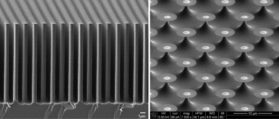
General device patterning, optical device etching, waveguides, metamaterials patterning, fluidics platforms, pillar arrays, dry etch release of cantilevers.
A wide variety of structures are enabled by RIE.

Specifications
- LN2-cooled/heated electrode (-150 to +400 °C)
- 3000 W or 5000W ICP RF generator
- 600 W lower electrode (Bias) RF generator
- 4” wafer processing down to small chips
- 4” cross wafer etch uniformity typically <+/-5%
- Anisotropic or isotropic etching
- Silicon etcher process gases: C4F8, SF6, CHF3, CF4, Ar, O2, N2
- Metal etcher process gases: BCl3, Cl2, CF4, CHF3, C4F8, SF6, H2, Ar, O2, N2
Contact Information
Dayrl P Briggs
Lead Cleanroom Engineer
[email protected]